


Gabor-filtering LSI modeling primary visual cortex function
-
Gabor filtering, which is a processing model of the primary
visual cortex, can extract local spatial frequencies of an
image. The extracted features are useful for different types of
image processing such as texture analysis, face recognition. An
advantage of the features is that they are hardly affected by
illumination change. We have proposed a pixel-parallel algorithm
for Gabor filtering using resistive networks, and a VLSI chip
implementing the algorithm has been developed based on our
merged analog/digital architecture.
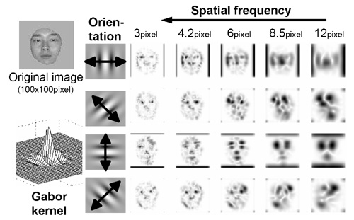
Image feature extraction by Gabor wavelet transforms (GWTs)
-
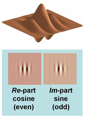
Gabor filtering is 2-D convolution with a kernel of cosine/sine waves
restricted by a Gaussian window.
-
Feature extraction of human face by GWTs
-
Gabor filtering is 2-D convolution with a kernel of cosine/sine waves
restricted by a Gaussian window.
Pixel-parallel Gabor-filter circuit and algorithm
- Conventional resistive network model used in Silicon Retina (C. Mead, 1988)
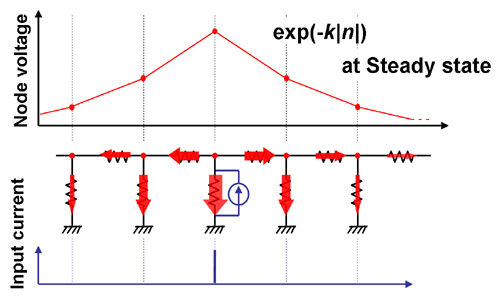
In this model, each pixel intensity is represented by a voltage (or current) source at each node of the network. The steady state of the network exhibits an exponential decay function as an impulse response. On the basis of this resistive network model, Gabor-like filtering circuits were proposed (B. E. Shi, 1998,1999).
- On the other hand, in our model, each pixel intensity is
represented by an initial charge at each node. The processing results
are given by a transient charge distribution of the nodes, which
exhibits a Gaussian function.
Our resistive network model
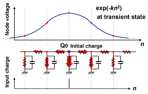
We have modified Shi's network based on the proposed network model. The realized window function of the kernel is Gaussian, and it leads to real Gabor filtering.
Pixel circuit for Gabor filtering based on the proposed model
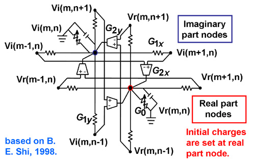
In our model, as time passed, charges diffuse, and node voltages abruptly decreases. Thus, we can only obtain Gabor coefficients with a very small average amplitude when a wide-spreading kernel is used. This also degrades calculation precision for LSI implementation with fixed-point arithmetics.
To overcome this difficulty, we propose another modification. In the proposed circuit, conductance (G0) between each node and the ground only affects the relative amplitude of whole pixel nodes, and it never modifies the kernel shape. if G0 is negative, then the node values are amplified as time passes because G0 acts as negative conductance. Therefore, in our improved model, by changing the value of G0, or by alternately reversing the sign of G0 appropriately, we can obtain Gabor kernels with a predefined peak amplitude. Obviously, we can use an appropriate value of G0 for obtaining the predefined peak amplitude, but the appropriate value seems to be critical. Changing the sign of G0 is a more controllable method.
- Conventional resistive network model used in Silicon Retina (C. Mead, 1988)
Design of pixel-parallel Gabor-filtering LSI based on merged A/D approach
-
It is difficult to implement the resistive networks with precise
transient state control by pure analog approach. We use a merged A/D
approach using PWM signals to emulate analog circuit operation by
discrete-time operation. Voltage change in each node is calculated
using Kirchhoff's law.
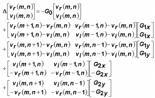
Node-voltage updating equations based on the proposed Gabor-filtering circuit
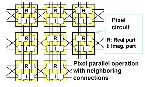
Pixel-parallel VLSI architecture
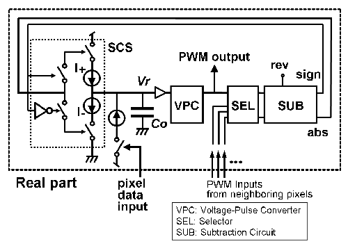
Pixel circuit based on merged A/D architecture
-
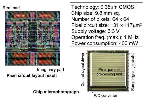
Pixel circuit layout and chip photograph of Gabor-filtering LSI
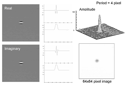
- Measurement results of fabricated Gabor-filtering LSI
Impulse response
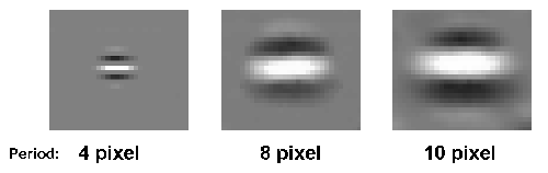
Impulse response of various periods
-
It is difficult to implement the resistive networks with precise
transient state control by pure analog approach. We use a merged A/D
approach using PWM signals to emulate analog circuit operation by
discrete-time operation. Voltage change in each node is calculated
using Kirchhoff's law.
VLSI Gabor-filtering system
- A system has been constructed by combining a PC and an FPGA board
controlling the fabricated Gabor-filtering LSI.
System configuration
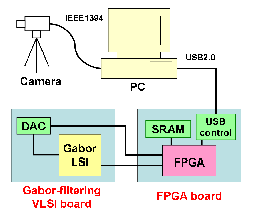
VLSI Gabor-filtering system
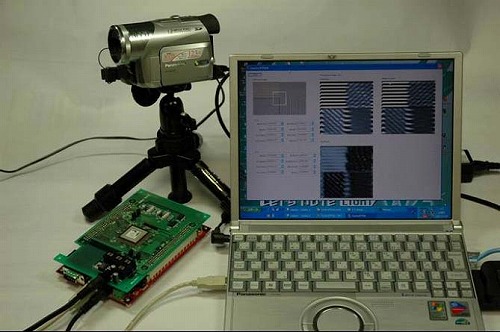
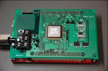
Gabor-filtering LSI board
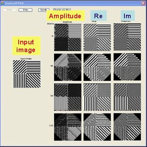
Output of VLSI Gabor-filtering system (PC display image)
Stripe patterns with vertical, horizontal, and oblique angles are extracted.
- A system has been constructed by combining a PC and an FPGA board
controlling the fabricated Gabor-filtering LSI.